
How to Ensure a Via in Pad is Reliable
Via in Pad
Via in pad is a popular method to increase component density and reduce signal loss on PCBs. However, if the via isn’t properly designed or manufactured it can lead to poor solder connections and failure under stress. So how do you ensure a via in pad is reliable?
In order for a via in pad to be reliable the drilled hole must be completely filled and capped. This is because solder can wick into the via and create voids that affect the quality of the solder joint. Solder voids reduce the electrical and thermal conductivity of the connection and are particularly problematic for high reliability applications like aerospace or medical devices.
When designing a via in pad with via in pad it is important to follow recommendations from component manufacturers on the placement of their pads and the appropriate size of the holes for those pads. Additionally, designers should choose the proper filling and capping methods. Conductive epoxy filling can prevent solder wicking, while copper capping improves solderability and helps to dissipate heat.
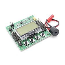
How to Ensure a Via in Pad is Reliable
Another important consideration is the proper choice of a PCB manufacturer for your project. Choosing a reputable PCB manufacturer with experience using via in pad can help you avoid manufacturing defects and improve your yield. They will be able to advise you on the best drilling technique and via type for your design and can run detailed design for manufacturing checks to identify and address any manufacturability issues.
One of the primary drawbacks of via in pad is that it takes longer to assemble a board with them than with standard vias. This is because the drilled hole must be plugged and then plated over, which adds to the overall manufacturing time of the board. Additionally, due to the inherent wander of a CNC drill, there may be a small annular ring around the drilled hole that must be capped.
It is also important to consider the materials used in a PCB when creating a via in pad. Resin filled vias are commonly used when the via serves as a mechanical conduit but does not need to conduct electrical signals. Electroplated vias, on the other hand, are a great option when you need to maintain electrical continuity.
Finally, it is important to optimize the number of vias on a PCB layout. Using only the necessary vias helps to reduce the length of the signal path and inductive and capacitive parasitics. Additionally, ensuring that vias are connected to large ground or power planes will help to dissipate heat.
By following the guidelines above, you can successfully use via in pad to increase component density and improve signal integrity. However, if the process is not carefully managed it can lead to poor solder joints and a decreased lifespan for the entire assembly. So if you’re looking for the best way to increase the efficiency and performance of your circuit board, consider using via in pad. Just make sure to work closely with your fab shop to ensure the process is done correctly!